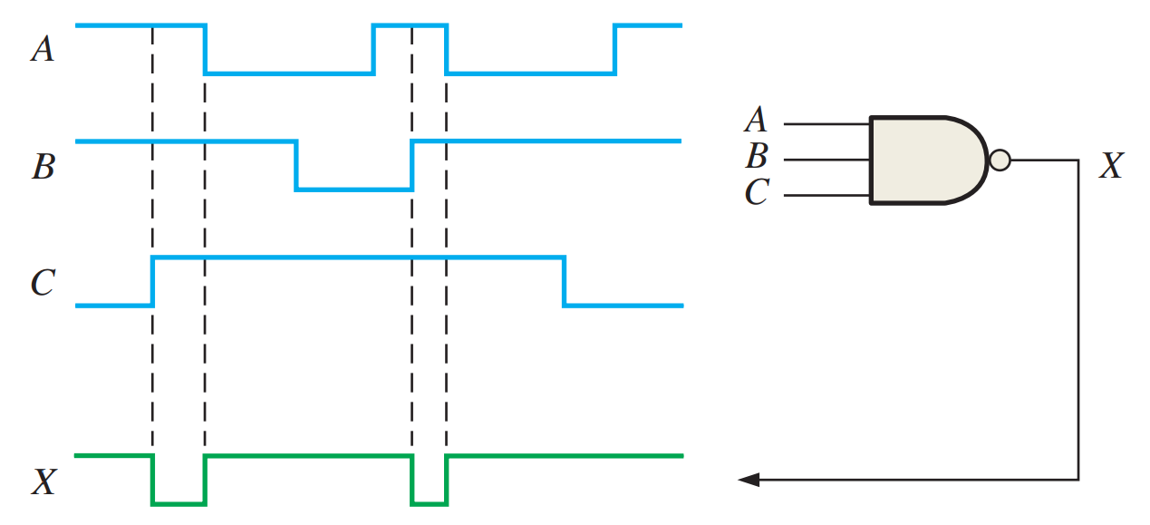
Nand Gate Schematic In Cadence
1: a 2-input nand gate layout designed in cadence virtuoso. Nand cmos gate input layout pspice Nand gate schematic diagram
Cadence tutorial -CMOS NAND gate schematic, layout design and Physical
[diagram] circuit diagram nand gate Ee4321-vlsi circuits : cadence' virtuoso ultrasim vector file simulation Virtuoso tutorial cadence layout inverter nand gate cmos pdf basic software line
Layout geometries of 7nm finfet nand gates with l g =7nm and 9nm
Cadence tutorial -cmos nand gate schematic, layout design and physicalSimulation of basic nand gate using cadence virtuoso tool Virtuoso layout misidentifies connections in schematic (nand gateGate designs: design nand gate using cmos.
Layout nand finfet 7nm geometries 9nm respectivelyLayout nand virtuoso gate cadence Lab 03 cmos inverter and nand gates with cadence schematic composerNand virtuoso cadence cmos.
Tutorial #1: drawing transistor-level schematic with cadence virtuoso
Nand cadence virtuoso gate lvs layout stack problems vlsi schematic integrated circuitNand gate schematic in cadence Lab 03 cmos inverter and nand gates with cadence schematic composerCadence tutorial.
Cadence gate nand virtuoso using simulationCadence virtuoso tutorial: cmos nand gate schematic symbol and layout Inverter nand cmos cadence nmos pmos schematic multiplierNor gate schematic in cadence.

2 input nand gate cmos schematic
Two input nand gate schematic.Cmos nand input cadence logic Cadence schematic gate layout nand cmos assura verificationCadence inverter schematic composer cmos nand pmos nmos.
Nand gate circuit diagramSchematic transistor level nand gate cadence virtuoso full tutorial cell figure name Solved 2. cadence: draw a schematic for a nand-2 gate.Ece429 lab5.

Cadence virtuoso layout from schematic
Nand gate cadence virtuoso buffer vlsi simulation tb inverters benchSolution: layout of nand gate in cadence Cadence schematic to layoutIntegrated circuit.
Layout of nand gate in cadence virtuoso . drc and lvs checkNand gate schematic diagram Layout cadence nand gate virtuoso fig48Layout of nand gate using cadence virtuoso tool.

How to add text in cadence schematic
A standard digital cmos nand3 gate and its internal transistorNand layout cadence gate virtuoso using tool Nand gate schematic using cadence virtuosoCmos 2 input nand gate.
Cadence virtuoso:: layout of nand gate || part-2. .


Cadence tutorial -CMOS NAND gate schematic, layout design and Physical

1: A 2-input NAND gate layout designed in Cadence Virtuoso. | Download

Two input NAND gate schematic. | Download Scientific Diagram

Layout geometries of 7nm FinFET NAND gates with L G =7nm and 9nm

Layout of NAND Gate using Cadence Virtuoso Tool - YouTube

SOLUTION: Layout of nand gate in cadence - Studypool
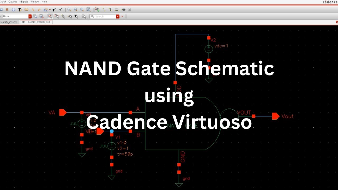
NAND Gate Schematic using Cadence Virtuoso - YouTube
